In electronics, adder circuit performs addition of the binary numbers.in various computers and other types of processors. Adder circuits are not only used in ALUs, but also used in various processors to calculate increment or decrements operations, table indices, addresses, etc. A typical adder circuit generates sum and carry as the output. The main purpose of these addresses are used to add the different formats like XS-3, binary coded decimal (BCD) and gray code. When the one’s or two’s compliment are being used to specify negative numbers, it is small to alter adder to subtractor. A more complex adder is used to represent other signed numbers. The applications of adder circuit are, adder circuits are not only used to add binary numbers, but also used in digital applications such as address, table index, decoding and calculation etc.
Types of Adder Circuits
Adder circuits are classified into two types, namely Half Adder Circuit and Full Adder Circuit
Half Adder Circuit
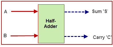
The half adder circuit is used to sum two binary digits namely A and B. Half adder has two o/ps such as sum and carry, where the sum is denoted with ‘S’ and carry is denoted with ‘C’. The carrier signal specifies an overflow into the following digit of a multi-digit addition. The value of the sum ‘S’ is 2C+S. The simplest design of half adder is shown below. The half adder is used to add two i/p bits and generate a sum and carry which are called as o/ps. The i/p variables of the half adder are termed as augend bits & addend bits, whereas the o/p variables are termed as sum and carry.
half adder circuit
Truth Table of Half Adder
The truth table of half adder is shown below, using this we can get the Boolean functions for sum & carry. Here Karnal map is used to get the Boolean equations for the sum and carry of the half adder.
truth table of have adder
Half Adder Logic Diagram
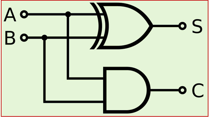
The logic diagram of half adder is shown below.If A & B are binary i/ps of the half adder, then the Boolean function to calculate the sum ‘S’ is the XOR gate of inputs A and B. Logic functions to calculate the carry ‘C’ is the AND gate of A and B. From the below half adder logic diagram, it is very clear, it requires one AND gate and one XOR gate. The universal gates, namely NAND and NOR gates are used to design any digital application. For example, here in the below figure shows the designing of a half adder using NAND gates.
logic diagram for half adder
VHDL Code For Half Adder
entity ha is
Port (a: in STD_LOGIC;
b : in STD_LOGIC;
sha : out STD_LOGIC;
cha : out STD_LOGIC);
end ha;
architecture Behavioral of ha is
begin
sha <= a xor b ;
cha <= a and b ;
end Behavioral
Full Adder Circuit
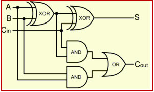
A full adder is used to add three input binary numbers. Implementation of full adder is difficult compared with half adder. Full adder has three inputs and two outputs, i/ps are A, B and Cin and o/p’s are sum ‘S’ and carry ‘Cout’. In three inputs of the full adder, two i/ps A B are addend and augend, where third i/p Cin is carry on preceding digit operation. The full adder circuit generates a two bit o/p and these are denoted with the signals namely S and Cout. Where sum= 2XCout+S.
full adder circuit
Truth Table of Full Adder
The truth table of full adder circuit is shown below, using this we can get the Boolean functions for sum & carry. Here Karnal map is used to get the Boolean equations for the sum and carry of the full adder.
truth table for full adder
Full Adder Logic Diagram
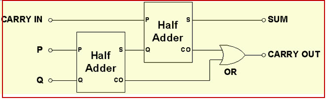
This full adder logic circuit is used to add three binary numbers, namely A, B and C, and two o/ps sum and carry. This full adder logic circuit can be implemented with two half adder circuits. The first half adder circuit is used to add the two inputs to generate an incomplete sum & carry. Whereas, a second half adder is used to add ‘Cin’ to the sum of the first half adder to get the final output. If any half adder logic circuit generates a carry, there will be an o/p carry. So output carry will be an OR function of the half adder’s carry o/p. Take a look at the full adder logic circuit shown below.
full adder logic diagram
The implementation of larger logic diagrams is possible with the above full adder logic a simpler symbol is mostly used to represent the operation. Given below is a simpler schematic representation of a one-bit full adder.
Full Adder Design Using Half Adders
With this type of symbol, we can add two bits together, taking a carry from the next lower order of magnitude, and sending a carry to the next higher order of magnitude. In a computer, for a multi-bit operation, each bit must be represented by a full adder and must be added simultaneously. Thus, to add two 8-bit numbers, you will need 8 full adders which can be formed by cascading two of the 4-bit blocks.
VHDL Coding for Full Adder
entity full_add is
Port ( a : in STD_LOGIC;
b : in STD_LOGIC;
cin : in STD_LOGIC;
sum : out STD_LOGIC;
cout : out STD_LOGIC);
end full_add;
architecture Behavioral of full_add is
component ha is
Port ( a : in STD_LOGIC;
b : in STD_LOGIC;
sha : out STD_LOGIC;
cha : out STD_LOGIC);
end component;
signal s_s,c1,c2: STD_LOGIC ;
begin
HA1:ha port map(a,b,s_s,c1);
HA2:ha port map (s_s,cin,sum,c2);
cout<=c1 or c2 ;
end Behavioral;
more links:- know the differences between cdma and gsm.
Social Media Influencers trace their root to the late 1700s when influencer marketing originated and has evolved to become the main kind of influencer marketing today, with a worth…
INSIGHTS
The total market size (revenue) of the wholesale footwear market in 2018 is $38 billion, with expected revenue growth of 2% in 2019.
The key players in the athletic appar…
PepsiCo's CEO, Indra Nooyi, is creating a culture of gender equality through several initiatives that support women throughout the world, both among PepsiCo employees and in the…
INSIGHTS
Texas Instruments saw a 23% increase in revenue following the launch of its creative branding strategy for its Medical Business Unit.
Qualcomm's average monthly website …
INSIGHTS
Some people deny global warming exists due to inaccurate temperature data and unreliable climate models.
The belief that climate change is an expected and natural part of…
INSIGHTS
The ways global warming can be combated include promoting terrestrial carbon dioxide removal, photocatalysis of non-CO2 greenhouse gases, using renewable energy sources, …